Did you already switch the BOOT1 jumper?
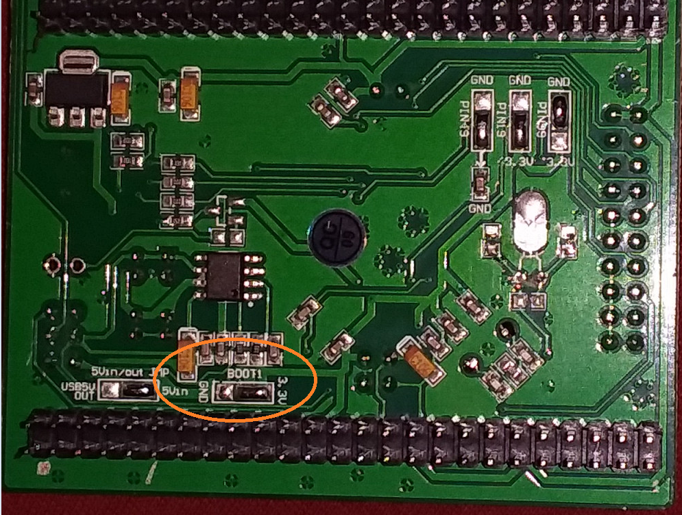
How is the chip IC3? Are any of the control signals shorted to the 0V pads?

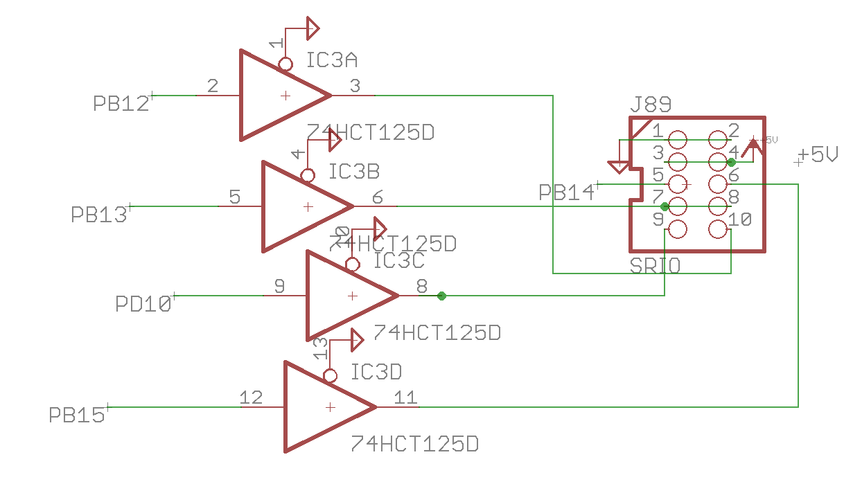
Here’s a schematic snip of the same thing connected to J89. You can also read back the signals to the MCU pins from this chip, namely PB12, PB13, PD10 and PB15
What happens if you connect the J89 cable to another neo board?
Can it be that the micromatch headers are the wrong way around? There is a slot that permits the cable going in only one way but some connectors have a slot on both sides. Still, the PCB would prevent improper insertion as long as the cable was wired correctly.
Maybe post a picture of the neo boards too, especially of the ICs.